Optospintronic Devices
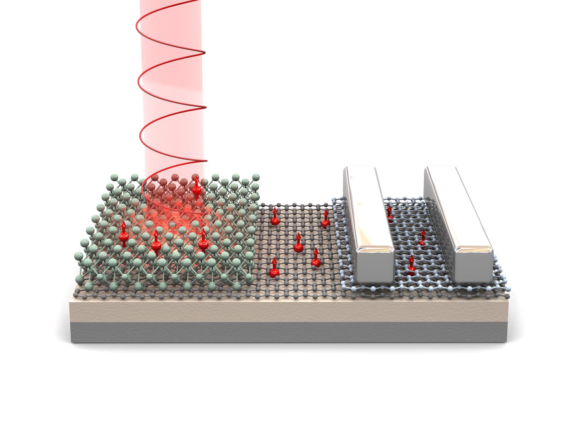
We demonstrated the possibility of direct, nondestructive optical spin injection into graphene by utilizing the unique spin-valley physics of 2D semiconducting monolayers. Our approach used circularly polarized light to selectively address the carrier valley degree of freedom in a monolayer WSe2 crystal. Due to the broken inversion symmetry and strong spin-orbit coupling, this process leads to a non-equilibrium spin concentration that tunnels into an adjacent graphene layer.
This work established a new functional regime for optospintronic devices, where spin information is generated optically and transported over long distances—up to 3.5 μm—within the graphene channel. It also provides a scalable framework for 2D spintronic logic gates. This enables the seamless integration of optical communication with spin-based memory and computation, potentially leading to hybrid opto-electronic-spintronic processors that are immune to typical electronic interference and heat dissipation issues.
Project Technical Profile
Core Skills: Spintronics, Optospintronics, Nonlocal Spin Transport, vdW Heterostructure Assembly.Key Achievement: First demonstration of optical spin injection in graphene via proximity coupling with a 2D semiconductor.