Hi, I'm Dimitri
I am an R&D leader and scientist with a PhD from EPFL, specializing in the development of next-generation optoelectronics and semiconductor products.
With 6 years in industrial R&D management and 7 years of academic research, my career spans from pioneering fundamental research of quantum phenomena in 2D materials to building and managing diverse cross-disciplinary teams and driving product development from POC to industrialization in the field of optics, electronics, renewable energy and quantum devices.
I thrive at the intersection of complex problem-solving, innovations and industrialization, bridging the gap between scientific breakthroughs and scalable hardware solutions.
Head of the Optical Innovations R&D division, leading a 30-member organization (5 teams, 7 direct reports). Directed the end-to-end development of 5 product lines across semiconductor physics, optics, and renewable energy, bridging the gap between high-level strategy and technical execution.
Click on the role to see more details
Strategic Leadership & Operations:
- Steered the company’s IP strategy and managed an extensive patent portfolio to protect core engineering innovations.
- Initiated and executed various initiatives fostering innovation, aligning product development with company goals, improving delivery quality, and maintaining investment discipline.
- Implemented an OKR framework and improved performance review systems, resulting in higher delivery quality and shortened R&D cycle times.
- Led full-cycle talent management from hiring and onboarding to creating individual growth plans and cross-team 'chapters' to foster a culture of innovation.
Technical Direction & Stakeholder Management:
- Served as the primary Technical Lead and Subject Matter Expert in Optics, Imaging and semiconductor physics, providing deep-dive technical guidance to engineering teams.
- Orchestrated complex collaborations with NRE partners, suppliers, research institutions, and independent consultants to accelerate growth and ensure long-term competitiveness.
- Ensured all products met rigorous industry standards, certifications, and security regulations from design to delivery.
- Acted as a link between R&D, Executive Management, and Product teams to ensure operational alignment and technical feasibility.
Built and guided a 12-member multidisciplinary team of scientists and engineers to drive product development from POC to EVT. Took full ownership of system-level integration, balancing cutting-edge technical specifications with aggressive size constraints and industrial cost targets.
Click on the role to see more details
- Recruited and mentored a high-performing team of scientists (optics, material, chemistry, semiconductor physics), hardware engineers (optical, mechanical, electrical), and software developers (firmware, algorithms).
- Took full ownership of product evolution, delivering 5 generations of prototypes and a fully optimized system within a 24-month window.
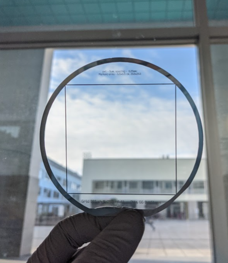
- Led the development of an ultra-transparent conductive coating that outperformed current state-of-the-art industry benchmarks.
- Drove seamless integration across hardware, algorithms and software stacks, implementing custom data and image processing workflows to accelerate iterative R&D cycles.
- Managed a 2-year, $0.5 M federal-grant collaboration with CSEM, aligning academic research with commercial product goals.
- Co-authored multiple patent filings, securing system-level innovations and protecting proprietary engineering architectures.
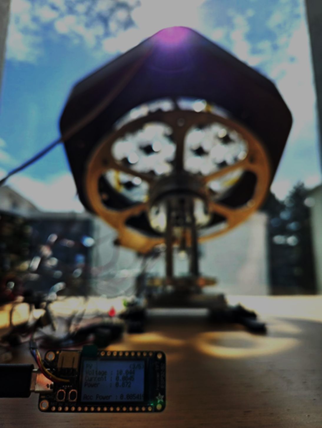
Conceived and prototyped a novel photovoltaics product, securing budget and resources for further development.
Click on the role to see more details
- Engineered a novel optical positioning system within six months, independently managing the optical design, mechanical CAD, and computer vision algorithm development.
- Achieved 2x increase in organic PV cell efficiency by optimizing device architecture, material selection, and fabrication processes.
- Accelerated internal R&D by providing advanced theoretical analysis and numerical simulations for complex thin-film coatings to other teams.
- Safeguarded core innovation by drafting and filing a foundational patent application.
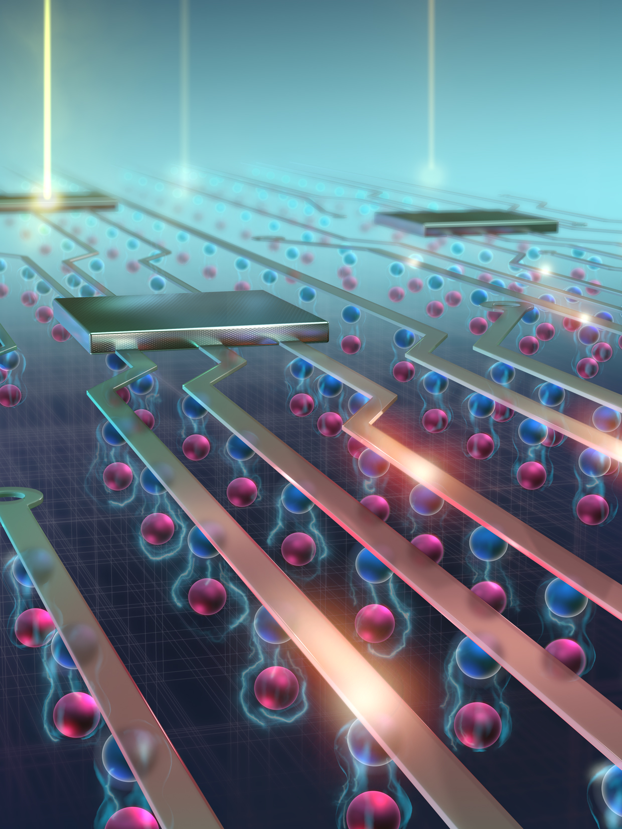
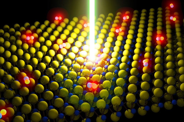
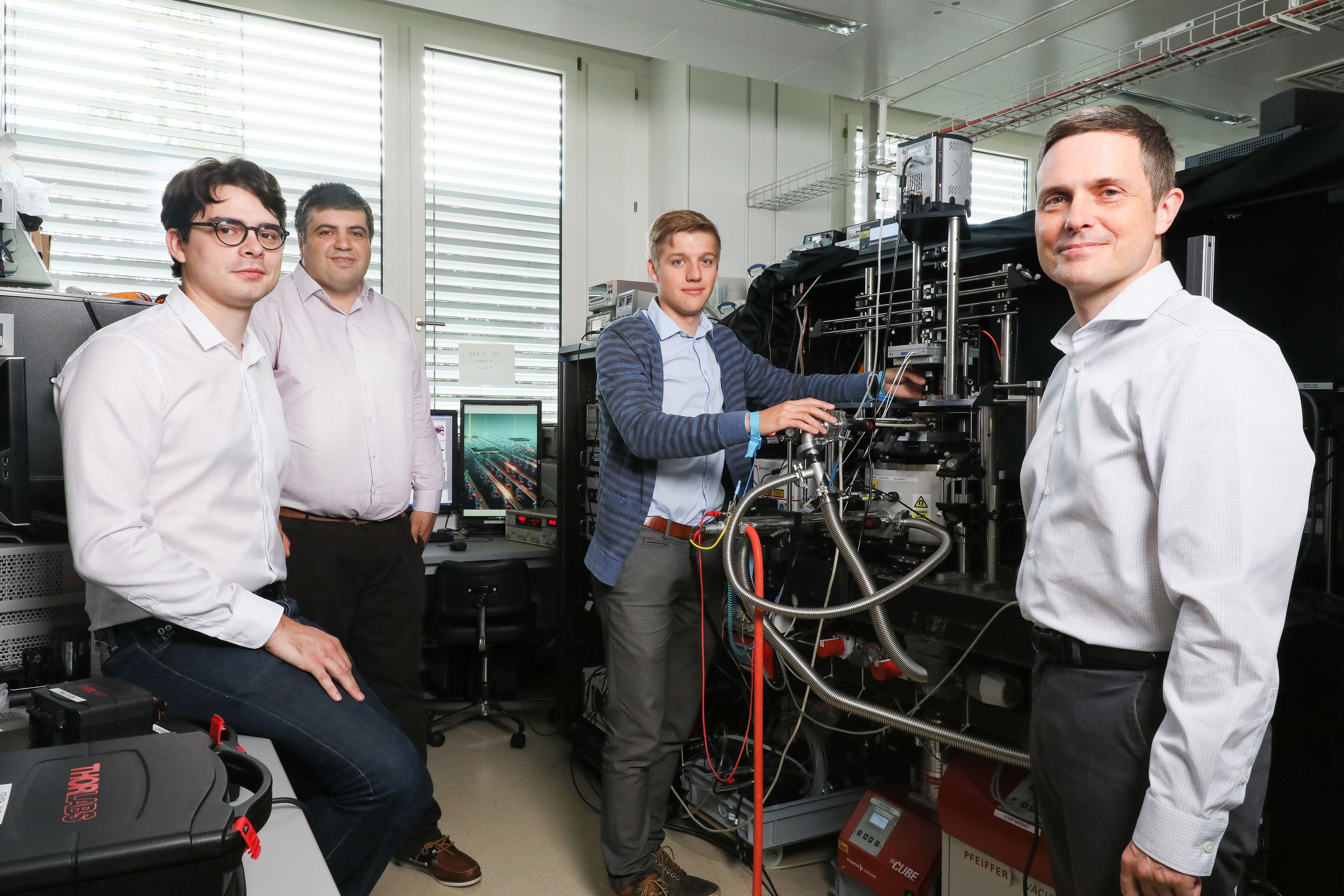
Research of quantum phenomena in 2-dimensional systems.
Click on the role to see more details
Main Achievements:
- Demonstration of the first excitonic transistors operational at room-temperature.
Outcomes:
- 12 publications in high impact journals including Nature.
- 2 research awards and featuring in the Nature Photonics cover.
Other Projects:
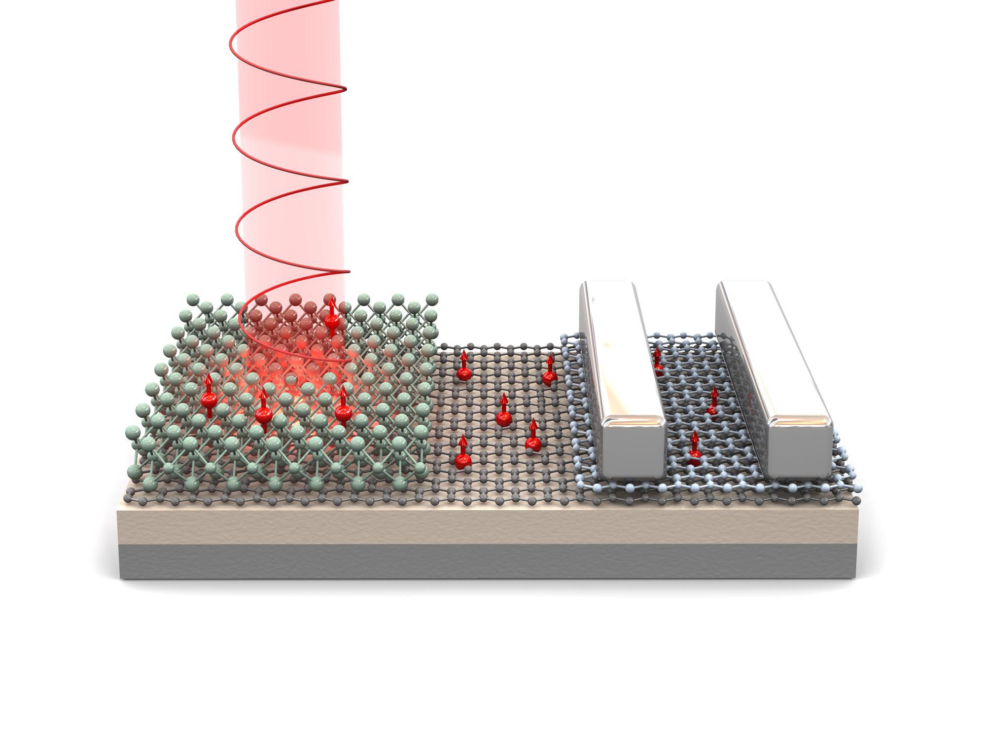
- Development of spintronic and opto-spintronic devices based on 2D materials.
- Development of the electrically pumped laser based on 2D materials.
- Integration of 2D LED/photodetector with waveguides and photonic cavities.
Key Responsibilities:
- Developing novel device architectures, numerical simulations, experiment design.
- Cleanroom microfabrication.
- Electrical transport and optical measurements.
- Designing and assembling cryogenic setups.
- Mentoring master and PhD students.
- Teaching 'Measuring Systems' course for EPFL master students.
Extracurricular
Conceptualized and developed a specialized, non-commercial AI research platform designed to optimize athlete performance through data-driven nutrition modeling and personalized counseling.
Click on the role to see more details
- Architected specialized nutrition algorithms tailored for high-performance athletic requirements.
- Integrated multimodal inputs and LLM-based advisory tools for data-driven nutrition coaching.
- Built cross-platform iOS and Android applications to deliver personalized insights and tracking to athletes.
- Delivered personalized insights and nutrition counseling via a streamlined user interface.
- Maintaining the project as a non-revenue-generating venture.
- Exploring the intersection of machine learning and sports science.
Supported the education of future engineers through hands-on lab supervision and theoretical guidance for 'Measuring Systems' course for EPFL master students.
Click on the role to see more details
- Supervising and guiding electrical engineering students.
- Conducting theoretical and experimental classes.
- Prototyping on NI ELVIS board and LabVIEW programming.
Led the organization of an international summer school 'Optoelectronics on 2D materials', managing fundraising, logistics, and program curation.
Click on the role to see more details
- Fundraising (CHF 40k), sponsorship search, and venue arrangement.
- Speakers selection, invitation, and their travel arrangement; participants selection.
- School promotion, website and school’s design development.
Served as a jury member for the final round, evaluating theoretical and experimental works.
Click on the role to see more details
- Organization of theoretical and experimental rounds.
- Correcting and grading participants' works including tête-à-tête appeals.
Counseled high school students and corrected physics and mathematics assignments.
Click on the role to see more details
- Students distance learning counseling and correction of their works.
Doctoral degree in optics and nanoelectronics of low dimensional systems.
- Thesis: Spin-valley optoelectronics based on 2D materials.
- Doctoral school of Microsystems and Microelectronics (EDMI) at EE department.
- Recipient of two awards for outstanding thesis.
M1 'Physics for Optics and Nanosciences' and M2 'Nanosciences'.
- Thesis: Synthesis and characterization of nanostructured materials.
- Ranked 1st in the class. GPA: 3.91/4 (M1), 3.81/4 (M2).
- M1 and M2 Internships "Characterisation of nanoclusters deposited on graphene and carbon nanotubes." at Paris Sud University, Laboratoire Aimé Cotton.
Physics and Technology of Nanostructures.
- Diploma with high honors. GPA: 4.94/5.
- Faculty of General and Applied Physics.
- 2013 Internship "Crystallization of membrane proteins for structure analysis" at Institute for Biophysics, Heinrich Heine University, Düsseldorf, Germany.
- 2012 Internship "Structural analysis of beta-amyloid fibrils" at Institute of Complex Systems, Forschungszentrum, Jülich, Germany.
Languages
Technical Skills
Cryogenics
Electrical Transport
Optical Measurements
Clean Room Microfabrication
Metrology / Characterisation
Computer Skills
Programming & Tools
Numerical Simulations
Design Tools
Room-temperature electrical control of exciton flux in a van der Waals heterostructure
Valley-polarized exciton currents in a van der Waals heterostructure
Polarization switching and electrical control of interlayer excitons in two-dimensional van der Waals heterostructures
MoS2 photodetectors integrated with photonic circuits
Optospintronics in Graphene via Proximity Coupling
Room-temperature electrical control of polarization and emission angle in a cavity-integrated 2D pulsed LED
Layer-modulated magnetism in two-dimensional metallic PtSe2
Keynote speaker at internal conferences
Electrostatic control of exciton flux in van der Waals heterostructures
Control of interlayer excitons in two-dimensional van der Waals heterostructures
Reconfigurable Diodes Based on Vertical WSe2 Transistors with van der Waals Bonded Contacts
Optospintronics in Graphene via Proximity Coupling
Atomically thin electrically tunable light-emitting diodes

Multilayer Electronic Device and Method for Producing the Same
Process of signing documents
Dispersive optical device, dispersive optical system comprising the same
Sunlight steering apparatus and solar energy harvesting system comprising the same
Light collecting assembly
Optical system for a position determination device
Method of detecting and processing spatially-distributed two-dimensional markers
METHOD OF ADJUSTING A FOCUSING DISTANCE OF AN OPTICAL SENSING SYSTEM
Excitonic device and operating methods thereof
Scientific recognition:
Scholarships:
Awards:
Science Olympiads Medals:
Key Projects & Innovations

* A few other exciting projects are under NDA.